
Chapter 1 Introduction to Versal#
Versal includes Cortex-A72 processor and Cortex-R5 processor, PL programmable logic part, PMC platform management controller, AI Engine and other modules are different from the previous ZYNQ Unlike MPSoC 7000, Versal is interconnected internally through the NoC on-chip network.

Overall block diagram of the Versal chip
PS: Processing System is the part of ARM SoC that has nothing to do with FPGA.
PL: Programmable Logic, which is the FPGA part.
NoC architecture#
Versal programmable network-on-chip (NoC) is an AXI interconnect network used to share data between programmable logic PL, processor system PS, etc. The previous Versal series used the AXI cross-interconnect module, which is Versal’s the difference.
NoC is designed for scalability. It consists of a series of interconnected horizontal (HNoC) and vertical (VNoC) paths supported by a set of customizable hardware implementation components that can be configured in different ways to meet design timing, speed and logic utilization requirements . The following is the structure diagram of the NoC

From the structure diagram of NoC, we can see that it mainly consists of NMU (NoC master units), NSU (NoC slave units), NPI (NoC programming interface), NPS (NoC packet switch). The PS side can connect to NMU and then access DDRMC through NPS connection. Similarly, the PL side can also access DDRMC through NMU and NPS. Access each module flexibly through NPS routing.

NMU structure
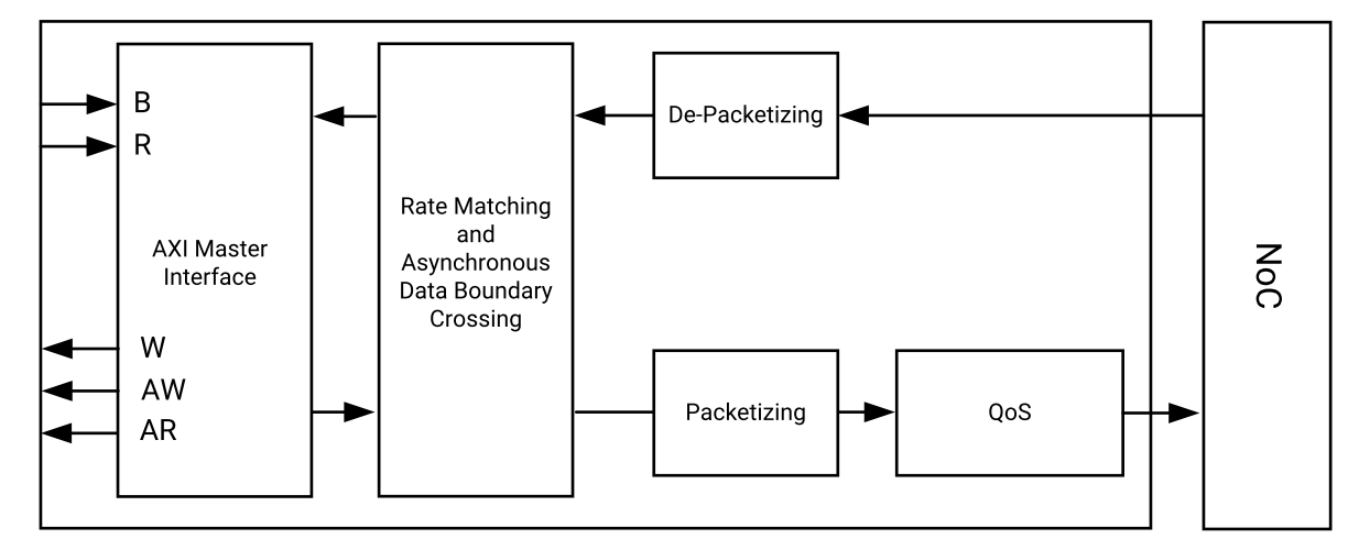
NSU structure
From the above NMU, It can be seen from the NSU structure that the interface to the user is still the AXI bus. Inside it, AXI data is packaged or unpacked and connected to the NoC network.

NPS structure
Both NMU and NSU are connected to the NPS, which is equivalent to a router and forwards data to the destination device. It’s a full 4x4 switch, each port supports 8 virtual channels in each direction, using credit-based flow control, similar to TCP’s sliding window.
NoC is a very important component in the development of Versal. The PS side accesses DDR and the PL side accesses DDR through NoC. Different from Versal, versal does not have a DDR controller on the PS side and all accesses through NoC. Therefore, understanding the NoC structure is It is necessary. For more information, please refer to the official pg313 document.
PMC architecture#
PMC (Platform Management Controller) manages the platform during startup, configuration, and operation. As can be seen from the structure diagram below, PMC consists of ROM Code Unit, Platform Processing Unit, PMC I/O It is composed of Peripherals and other units and has rich functions. Here we mainly introduce how PMC bootstraps startup.

PMC structure diagram

The first stage: Pre-Boot
PMC detects PMC power supply and POR_B release
PMC reads the boot mode pin and stores it in the boot mode register
PMC sends reset to RCU (ROM code unit)

The second stage: Boot Setup
RCU executes BootROM from RCU ROM
BootROM reads the boot mode register and selects the boot device
BootROM reads PDI (programmable device image) from the boot device and verifies it
7. BootROM releases the PPU reset, loads the PLM into the PPU RAM and verifies it. After verification, PPU wakes up and PLM The software starts executing.
BootROM enters sleep state

The third stage: Load Platform
PPU starts executing PLM from PPU RAM
PLM starts to read and run the PDI module
PLM uses PDI content to configure other parts of Versal
11a: PLM configures data for the following modules: PMC, PS clocks
(MIO, clocks, resets, etc.) (CDO file)
NoC initialization and NPI module (DDR controller, NoC,
GT, XPIPE, I/Os, clocking and other NPI modules
PLM loads the application ELF of APU and RPU into storage space,
Such as DDR, OCM, TCM, etc.
11b: PL side logic configuration
PL side data (CFI file)
AI Engine configuration (AI Engine CDO)
The fourth stage: Post-Boot
PLM continues to operate until the next POR or system reset. And responsible for DFX reconfiguration, power management, subsystemsRestart, error management, security services.
An introduction to the Versal chip development process#
Since Versal integrates the CPU and FPGA, developers need to design not only ARM operating system applications and device drivers, but also the hardware logic design of the FPGA part. During development, you need to understand the Linux operating system and system architecture, and you also need to build a hardware design platform between FPGA and ARM systems. Therefore, the development of Versal requires collaborative design and development by software personnel and hardware personnel. This is the so-called “software and hardware co-design” in Versal development.
The design and development of the hardware system and software system of the Versal system requires the following development environment and debugging tools: Xilinx Vivado. The Vivado design suite implements the design and development of the FPGA part, pin and timing constraints, compilation and simulation, and implements the RTL to bitstream design process.
Xilinx Vitis is the Xilinx software development kit (SDK). Based on the Vivado hardware system, the system will automatically configure some important parameters, including tool and library paths, compiler options, JTAG and flash memory settings, debugger connection and bare metal board support package (BSP). SDK is also available for all supported Xilinx The IP hard core provides drivers. Vitis supports collaborative debugging of IP hard core (on FPGA) and processor software. We can use high-level C or C++ language to develop and debug ARM and FPGA systems to test whether the hardware system is working properly. Vitis software also comes with Vivado software and does not need to be installed separately.
The development of Versal is also a hardware-first-software approach. The specific process is as follows:
Create a new project on Vivado and add an embedded source file.
Add and configure some basic peripherals of PS and PL in Vivado, or need to add customized peripherals.
Generate the top-level HDL file in Vivado and add the constraint file. Then compile and generate bitstream file ( XX.pdi).
Export the hardware information to the Vitis software development environment. In the Vitis environment, you can write some debugging software to verify the hardware and software, and combine the bitstream files to debug the Versal system alone.
Generate u-boot.elf and bootloader images in the VMware virtual machine.
Generate a BOOT.pdi file from the bitstream file and u-boot.elf file in Vitis.
Generate Ubuntu kernel image file Zimage and Ubuntu root file system in VMware. In addition, you need to write a driver for the FPGA’s custom IP.
Put the BOOT, kernel, device tree, and root file system files into the SD card, turn on the power of the development board, and the Linux operating system will boot from the SD card.
What skills are required to learn Versal?#
Learning Versal is more demanding than learning traditional tool development such as FPGA, MCU, ARM, etc. Learning Versal well is not something that can be accomplished overnight.
software developer#
Principles of computer composition
C, C++ language
Computer operating system
tcl script
Good foundation in English reading
logic developer#
Principles of computer composition
C language
Basics of digital circuits